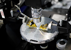
Optimizing Wide Bandgap Semiconductor Materials for Future Electronics
Introduction:
The rapid evolution of technology in the realm of power electronics has been significantly influenced by the emergence of Wide Bandgap (WBG) semiconductors. Silicon Carbide (SiC) and Gallium Nitride (GaN) are at the forefront of this revolution, promising enhanced performance in various applications, ranging from electric vehicles to industrial drives. This article delves into the meticulous process of discovering optimal materials for Wide Bandgap semiconductors, exploring the considerations, challenges, and advancements in the quest for superior electronic materials.
Understanding Wide Bandgap Semiconductors:
Wide Bandgap semiconductors, characterized by a larger energy bandgap than traditional silicon, exhibit unique electrical and thermal properties. These materials, such as SiC and GaN, enable high-frequency and high-temperature operation, contributing to increased efficiency and power density in electronic devices. The journey to discovering optimal materials for WBG semiconductors involves a multi-faceted approach encompassing materials science, engineering, and advanced characterization techniques.
Considerations in Material Selection:
-
Bandgap Engineering: The bandgap of a semiconductor is a crucial parameter influencing its electronic properties. Optimal materials for WBG semiconductors are those that possess a wide bandgap, allowing for higher breakdown voltages and reduced leakage currents. Researchers continuously explore new compounds and crystal structures to tailor bandgaps for specific applications.
-
Material Stability and Reliability: Ensuring the stability and reliability of materials under varying operating conditions is paramount. Wide Bandgap semiconductors must withstand high temperatures, voltage stress, and other environmental factors without compromising performance. Researchers focus on understanding material degradation mechanisms and developing solutions to enhance long-term stability.
-
Crystal Structure and Defects: The crystal structure of a semiconductor significantly impacts its electrical properties. Researchers investigate different crystal structures and work towards minimizing defects that can affect carrier mobility and introduce energy barriers. Advancements in crystal growth techniques and defect engineering contribute to optimizing material quality.
-
Carrier Mobility and Saturation Velocity: High carrier mobility and saturation velocity are key attributes for efficient electronic devices. Optimal materials for WBG semiconductors exhibit superior carrier transport properties, facilitating faster switching speeds and reduced power losses. Researchers explore doping strategies and material combinations to enhance carrier mobility.
Challenges in the Quest for Optimal Materials:
-
Material Processing Challenges: The synthesis and processing of WBG materials present challenges, especially when dealing with novel compounds or complex crystal structures. Researchers must develop scalable and cost-effective manufacturing processes to meet the demands of commercial applications.
-
Material Characterization: Accurate characterization of material properties is essential for understanding their behavior in electronic devices. Advanced techniques such as transmission electron microscopy, X-ray diffraction, and spectroscopy play a crucial role in unraveling the intricate details of WBG materials, but continual advancements are needed for even finer resolution.
-
Cost-Effectiveness: While the performance benefits of WBG materials are evident, cost considerations remain a significant challenge. The quest for optimal materials includes finding ways to reduce production costs through improved manufacturing processes, economies of scale, and the discovery of alternative materials with comparable performance.
Advancements and Future Directions:
-
Computational Approaches: Advances in computational materials science play a pivotal role in accelerating the discovery of optimal WBG materials. Quantum mechanical simulations and machine learning techniques enable researchers to predict material properties, guide experimental efforts, and explore a vast materials space efficiently.
-
Materials Genome Initiative: The Materials Genome Initiative (MGI) focuses on accelerating the discovery and deployment of advanced materials. In the context of WBG semiconductors, MGI supports collaborative efforts between academia, industry, and government to streamline the materials development process and bring innovative materials to market faster.
-
Interdisciplinary Collaboration: The interdisciplinary nature of materials discovery requires collaboration across various scientific and engineering disciplines. Collaborative efforts between physicists, chemists, engineers, and material scientists are essential for a holistic approach to optimizing WBG materials for diverse applications.
Conclusion:
The pursuit of optimal materials for Wide Bandgap semiconductors is a complex yet critical endeavor that underpins the future of power electronics. As researchers unravel the intricacies of material properties, address challenges in processing and characterization, and leverage computational tools, the potential for breakthroughs in WBG technology continues to grow. The collaboration between academia, industry, and government, coupled with advancements in materials science, holds the promise of unlocking new possibilities and transforming the landscape of electronic devices for generations to come.
Subscribe to Us !
-
 LV71081E-MPB-E
onsemi
-
 LMK00334RTVRQ1
Texas Instruments
-
 PI6C557-03LEX
Diodes Incorporated
-
 PCM1753DBQR
Texas Instruments
-
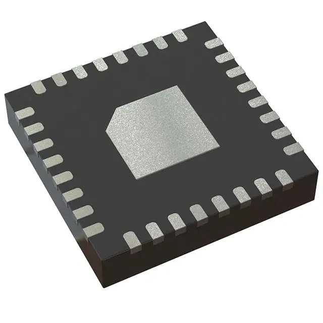 ADS1204IRHBT
Texas Instruments
-
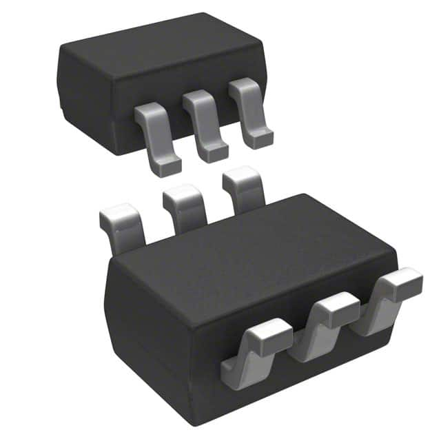 MCP4018T-104E/LT
Microchip Technology
-
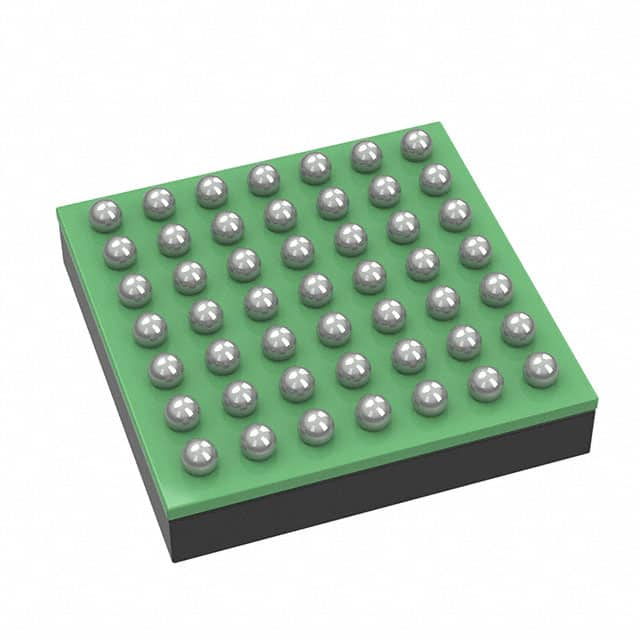 T4F49C2
Efinix, Inc.
-
.jpg) A40MX02-PLG44
A40MX02-PLG44Microchip Technology
-
 ATF16V8C-7PU
Microchip Technology
-
 SC-13048Q-A
GHI Electronics, LLC


