Transfer Learning Method for detailed defect classification in semiconductor manufacturing base
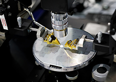
Defect Inspection and classification are the most crucial parts of manufacturing processes in semiconductor industries. Both these analyses are essential to identify and correct the processing problems to enhance the quality of the final product. A scanning electron microscope is the most widely used tool for process monitoring at production sites.
Defects in varied shapes and textures occur due to the complex manufacturing processes to develop enhanced semiconductors. It was found that when more manual processes were used, the number of defects increased and henceforth Automatic defects classification was developed. This was a function that automatically classifies defect images into predetermined defect classes. After ADC, Deep learning technology brought further essential improvements in defect classification by providing advanced analytical tools for analyzing big data from manufacturing. However, this technique required expensive ground truth labeling which was not always accurate. Based on certain tests, the convolutional neural network(CNN) transfer learning method (a deep learning technology) was considered the best method for defect classification.
Examined Defects
The process of examining defects starts with the engineers identifying the reasons for yield reduction from the results of examining defects. Defect analysis also helps to prevent defects from occurring again by adopting various measures. The main goal based on the analysis is to identify the root cause of commonly occurring defects and develop solutions.
During the course of this analysis of semiconductor manufacturing, defect images are categorized according to the class of defects to suppress yield reduction. Fig 1. showcases the various kinds of defects and Fig 2. shows that the examination of defects falls into three phases: classification of defects, monitoring trends in defects, and detailed analysis of classification. The specific frequency of a defect captured by using a scanning electron microscope (SEM) plays a crucial role to classify the defect type. Such trend monitoring is highly costly, hence deep learning technologies are used for the analysis of the defects.

Fig 1: Example of Defects

Fig 2: Overview of Defect Quality Control
Literature review
Many Scientists and researchers who were working to find a method for defect analysis found CNN (Convolution Neural Network) as the most efficient and effective method. Human-level classification can be achieved by using CNN due to its advanced analytical tools. Surface and fabric defect classification of steel sheets were introduced in the manufacturing sector which impacted globally for manufacturing. It ensures the high quality and performance of the products. Furthermore, effective features were extracted by a CNN-based defect image classification model through silicon processes.
It was commonly observed that supervision was adopted since a large set of data was inaccurately and manually labeled. This supervision approach for the transfer learning method is further explained below in the classification of defects and transfer learning method.
Classification of defects
A model was developed with an input SEM size of 128X128. The convolution factorization method was adopted to lower the computational cost where 1X1 convolutional layers were added before 3X3 convolutional layers to limit the number of input channels. This model consists of 33 convolutional layers with rectified linear activation in each layer. Fully connected layers are added after dropout and convolutional layers with sizes of 256 and defect class and finally, a softmax layer is added for outputting class probability calculation.
Pre-training and fine-tuning methods are the two foremost stages implemented for the model. The CNN model is trained from incorrectly stacked images (tens to thousand) to weakly supervised training in the pre-training stage. In the fine-tuning method, there is an extension of the output layer with randomly initialized weights so as to reduce the loss on the target task with fewer data points.
For evaluating the functioning of the Automatic Defect classification (ADC) method and the given method, water surface defect SEM images were examined from a manufacturing facility. In this experiment, four defect image datasets were assembled and each data set was marked noisy by non-experts and pure data by experts.
Fig 3 shows the comparison of the ADC method and the proposed method which concludes that the deep learning method is more effective than the traditional ADC method. Table III gives an analysis of per-class classification precision, recall, and sample count for every defect of set C.

Fig 3: Comparison of ADC and proposed methods
Transfer Learning Method:
Transfer learning means learning new tasks by relying on the previously learned tasks in a faster and more accurate way with less training data. Therefore, the Transfer Learning Method is used for the Highly accurate classification of defects. Fine-grained defects occur very rarely which is merely impossible to classify by manual classification methods. To classify such problems, a transfer learning strategy is adopted. There are 4 ways to approach this method based on what we want to transfer (1) Examination-based, (2) feature-based, (3) parameter-based, and 4) Relational-based. The domain used for fine-grained defect classification in the third phase is the same as the domain one used for rough defect classification in the first phase for which a feature-based approach is preferred.
Conclusion
The CNN-based transfer learning method is effective in order to avoid inconsistent manual classification and higher costs. The defect analysis task helps in identifying the root cause behind yield reduction and helps in classifying defect images with high accuracy and lowering labor costs. The transfer learning method can be used instead of the deep learning method which requires large labeled training data sets.
When the results were obtained from real semiconductor fabrication data it was concluded that the proposed method is more reliable than others. This method required fewer labeled data sets. Also, there was a significant decrease in the amount of labor required for manual inspection work which is nearly two-thirds of traditional ADC systems.
Subscribe to Us !
-
 LV71081E-MPB-E
onsemi
-
 LMK00334RTVRQ1
Texas Instruments
-
 PI6C557-03LEX
Diodes Incorporated
-
 PCM1753DBQR
Texas Instruments
-
 ADS1204IRHBT
Texas Instruments
-
 MCP4018T-104E/LT
Microchip Technology
-
 T4F49C2
Efinix, Inc.
-
.jpg) A40MX02-PLG44
A40MX02-PLG44Microchip Technology
-
 ATF16V8C-7PU
Microchip Technology
-
 SC-13048Q-A
GHI Electronics, LLC
 Afrikaans
 Shqip
Shqip አማርኛ
አማርኛ العربية
 Հայերեն
 Azərbaycan dili
 Euskara
 Беларуская мова
 বাংলা
বাংলা Bosanski
 Български
 Català
 Cebuano
 Chichewa
 简体中文
简体中文 繁體中文
繁體中文 Corsu
Corsu Hrvatski
 Čeština
 Dansk
Dansk Nederlands
 English
 Esperanto
 Eesti
Eesti Filipino
 Suomi
Suomi Français
 Frysk
Frysk Galego
 ქართული
 Deutsch
 Ελληνικά
 ગુજરાતી
 Kreyol ayisyen
 Harshen Hausa
 Ōlelo Hawaiʻi
 עִבְרִית
 हिन्दी
 Hmong
Hmong Magyar
 Íslenska
 Igbo
Igbo Bahasa Indonesia
 Gaeilge
 Italiano
 日本語
日本語 Basa Jawa
 ಕನ್ನಡ
ಕನ್ನಡ Қазақ тілі
 ភាសាខ្មែរ
 한국어
한국어 كوردی
كوردی Кыргызча
 ພາສາລາວ
 Latin
Latin Latviešu valoda
 Lietuvių kalba
 Lëtzebuergesch
 Македонски јазик
 Malagasy
 Bahasa Melayu
 മലയാളം
 Maltese
 Te Reo Māori
 मराठी
मराठी Монгол
 ဗမာစာ
ဗမာစာ नेपाली
 Norsk bokmål
 پښتو
پښتو فارسی
فارسی Polski
 Português
 ਪੰਜਾਬੀ
 Română
 Русский
 Samoan
 Gàidhlig
 Српски језик
 Sesotho
 Shona
Shona سنڌي
سنڌي සිංහල
සිංහල Slovenčina
 Slovenščina
 Afsoomaali
 Español
 Basa Sunda
 Kiswahili
 Svenska
 Тоҷикӣ
 தமிழ்
தமிழ் తెలుగు
 ไทย
ไทย Türkçe
 Українська
 اردو
اردو O‘zbekcha
 Tiếng Việt
 Cymraeg
 isiXhosa
 יידיש
יידיש Yorùbá
 Zulu
Zulu


